- INDEX目次
目次【非表示】
- 1.What Is Photoresist? A Photosensitive Material Essential for Semiconductor Manufacturing
- 2.The Role of Photoresist in Enabling Semiconductor Miniaturization
- 2-1.Step 1: Photoresist Coating on the Silicon Wafer
- 2-2.Step 2: Exposure — Transferring the Circuit Pattern
- 2-3.Step 3: Development and Etching — Removing Unwanted Areas
- 3.Main Types of Photoresist and Their Characteristics
- 3-1.Positive Photoresist — Exposed Areas Dissolve During Development
- 3-2.Negative Photoresist — Exposed Areas Harden and Remain After Development
- 4.Japan’s Photoresist Technology Supporting the Global Semiconductor Market
- 4-1.Reason 1: Advanced Quality Control Capable of Removing Impurities to the Absolute Minimum
- 4-2.Reason 2: A Domestic Supply Chain Covering Everything From Materials to Manufacturing Equipment
- 4-3.Reason 3: A Highly Detailed Development Framework That Responds Precisely to Customer Needs
- 5.Future Outlook and Emerging Technologies in Photoresists
- 5-1.The Potential Unlocked by Next-Generation Photoresist Technologies
- 6.Conclusion
- 7.Glossary Summary
Photoresist is a photosensitive material essential for semiconductor manufacturing.
This article explains its fundamental role and mechanism, as well as why Japanese technology is regarded as world-leading in this field.
Semiconductors are the backbone of modern society, and photoresist is crucial for forming their microscopic circuit patterns.
Japan’s advanced technology continues to support the evolution of the global semiconductor industry.
What Is Photoresist? A Photosensitive Material Essential for Semiconductor Manufacturing
Photoresist is a photosensitive material used to create patterns through light-induced chemical reactions. Its formulation consists of a polymer (resin), a photoactive compound, and a solvent. When exposed to light of a specific wavelength, the material undergoes a change in its chemical properties.
During development, either the exposed areas or the unexposed areas dissolve—depending on the resist type—allowing the intended pattern to remain.
By leveraging this behavior, photoresist functions as the “template” used to draw extremely fine electronic circuits onto a semiconductor substrate.
The Role of Photoresist in Enabling Semiconductor Miniaturization
Photoresist plays a central role in the photolithography process within semiconductor manufacturing. Photolithography is the technique of transferring circuit patterns onto a silicon wafer—the semiconductor substrate—using light.
During this process, the photoresist functions as a mask, allowing specific areas of the wafer to be protected or removed. Because the resolution of the circuit pattern directly depends on the performance of the photoresist, it is one of the most critical factors in achieving semiconductor miniaturization and higher device performance.
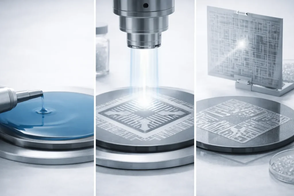
Step 1: Photoresist Coating on the Silicon Wafer
In semiconductor photolithography, the process begins by uniformly coating the silicon wafer—the base substrate—with liquid photoresist.
A device called a spin coater is used in this step. The wafer is rotated at high speed, and centrifugal force spreads the photoresist into an extremely thin, nanometer-scale film.
The more uniform this film is, the higher the accuracy of the circuit patterns formed later.
Therefore, the coating process is the first critical step that directly influences the overall quality of the semiconductor device.
Step 2: Exposure — Transferring the Circuit Pattern
After coating the wafer with photoresist, the process moves to the exposure stage, where the circuit pattern is transferred.
A photomask—an original plate containing the circuit design—is aligned over the wafer, and light from a source is projected through it.
Exposure systems use UV lasers such as i-line, KrF, and ArF, and as semiconductor miniaturization has progressed, shorter wavelengths have become essential. In cutting-edge manufacturing, EUV light with an even shorter wavelength is used.
The photoresist undergoes precise chemical changes in response to this light, allowing it to accurately record the photomask’s circuit pattern.
Step 3: Development and Etching — Removing Unwanted Areas
After exposure, the wafer is treated with a developer, which dissolves and removes the unwanted portions of the photoresist. This leaves behind a resist pattern that corresponds to the transferred circuit design.
Next, this resist pattern serves as a protective mask while the exposed areas of the silicon wafer are etched using chemicals or reactive gases. Once the circuit features have been engraved into the wafer, a stripping solution is used to completely remove the photoresist, which has finished its role.
Through this series of steps, the complex structures of a semiconductor chip are created.
Main Types of Photoresist and Their Characteristics
Photoresists are broadly classified into two types—positive and negative—based on how they respond to light.
This difference comes from how their chemical structure changes upon exposure.
Positive resists become soluble in the developer where light has struck, allowing those exposed regions to be removed. In contrast, negative resists harden when exposed to light, leaving the illuminated areas intact while the unexposed regions dissolve.
Because each type differs in characteristics such as resolution, cost, and chemical resistance, manufacturers choose between them based on the semiconductor device and application requirements.
Positive Photoresist — Exposed Areas Dissolve During Development
Positive photoresists undergo chemical decomposition in the areas exposed to light, making those regions more soluble in the developer.
As a result, the photomask pattern used during exposure is transferred to the wafer with high fidelity.
Because positive resists can reproduce mask shapes with exceptional accuracy, they offer very high resolution and are ideal for forming extremely fine circuit patterns. Today, positive photoresists are the dominant choice in advanced semiconductor manufacturing, including high-performance CPUs and memory devices.
Negative Photoresist — Exposed Areas Harden and Remain After Development
Negative photoresists behave opposite to positive resists: when exposed to light, they undergo a chemical reaction in which polymer chains crosslink and harden, making the exposed regions far less soluble in the developer.
Since the unexposed areas dissolve during development, the resulting resist pattern becomes a reversed, or “negative,” version of the photomask design.
Although negative resists generally offer lower resolution than positive resists, they provide advantages such as strong adhesion and excellent chemical resistance. They can also help reduce manufacturing costs, which is why they are used in specific semiconductor and electronic component production processes.
Japan’s Photoresist Technology Supporting the Global Semiconductor Market
In the global semiconductor market, photoresist is an essential material, and its overall market size continues to grow. In the field of high-performance photoresists—crucial for leading-edge semiconductor manufacturing—Japanese companies hold both strong technological advantages and a dominant market share.
For example, in EUV photoresists, Japanese manufacturers are said to hold virtually the entire global market. Across all photoresist categories, Japanese firms are estimated to supply roughly 50% to 80% of the world’s demand.
Major suppliers include JSR, Tokyo Ohka Kogyo (TOK), Shin-Etsu Chemical, Sumitomo Chemical, and Fujifilm. These companies play an indispensable role in supporting the global semiconductor supply chain.
Reason 1: Advanced Quality Control Capable of Removing Impurities to the Absolute Minimum
One reason Japanese companies maintain strong competitiveness in the photoresist market is their exceptional ability to remove impurities to the absolute minimum.
As semiconductor circuits shrink to the nanometer scale, even trace amounts of contaminants—such as metal ions or fine particulates—can lead directly to defects in the final product.
Japanese manufacturers leverage advanced synthesis and purification technologies developed through decades of research, enabling impurity control at the ppb level from raw materials all the way to finished products.
This uncompromising commitment to quality has earned them the trust of semiconductor makers around the world.
Reason 2: A Domestic Supply Chain Covering Everything From Materials to Manufacturing Equipment
Another major strength of Japan lies in its robust domestic supply chain.
Photoresist production requires highly specialized chemical materials—such as advanced polymers and photoactive compounds—and Japan is home to many leading chemical manufacturers capable of supplying these key components.
In addition, Japan also hosts world-class companies that produce the equipment used to coat, align, and expose photoresists on semiconductor wafers.
Because the entire ecosystem—materials, components, and manufacturing equipment—is concentrated within the country, companies can collaborate closely, enabling stable production of high-quality products and accelerating technological development.
Reason 3: A Highly Detailed Development Framework That Responds Precisely to Customer Needs
The performance requirements for photoresists vary greatly depending on the semiconductor type and the manufacturer’s production line.
Japanese photoresist makers excel because they maintain an exceptionally detailed development framework that can meet these diverse and highly specific customer demands.
Major companies such as Shin-Etsu Chemical, Fujifilm, and Sumitomo Chemical work closely with semiconductor manufacturers from the earliest stages of development. Through repeated cycles of prototyping and evaluation, they fine-tune (“co-develop”) products to achieve the exact properties needed for each process.
This customer-centric customization capability is a key source of Japan’s strong competitiveness in the global photoresist market.
Future Outlook and Emerging Technologies in Photoresists
The performance requirements of semiconductors will continue to rise, and photoresists—which support this evolution—must undergo further technological innovation.
As mass production of next-generation semiconductors using EUV (extreme ultraviolet) lithography accelerates, the global race to develop high-sensitivity photoresists capable of forming ultra-fine patterns with minimal light exposure is intensifying.
Companies in South Korea and Taiwan are also advancing development at a national level, and as reported in the news, a major question going forward is whether Japan can maintain its technological leadership in this field.
The Potential Unlocked by Next-Generation Photoresist Technologies
Research and development of next-generation technologies is underway to push beyond the limits of conventional photoresists as semiconductor miniaturization continues.
For example, because increasing the output of EUV light sources remains difficult, there is a growing need for high-sensitivity materials that can react efficiently even with minimal light exposure.
In response, new materials with mechanisms different from traditional chemically amplified resists are being developed, along with metal-containing resists that incorporate metallic elements. These emerging technologies can reduce line-width roughness (LWR) and enable more precise patterning, making them key to achieving semiconductor manufacturing at the 2-nanometer scale and beyond.
Conclusion
Photoresist is a key photosensitive material used to form the microscopic circuits of semiconductors, and its performance directly determines the overall quality of the chip.
In this market, Japanese companies—led by Tokyo Ohka Kogyo—continue to hold the top global share, driving the industry forward with their advanced technological capabilities.
Their ability to consistently develop and supply high-quality products exemplifies the strength of Japan’s manufacturing ecosystem.
Since the evolution of semiconductor technology is inseparable from innovation in photoresists, the stock performance and technological advancements of related companies will continue to draw significant attention across the industry.
Glossary Summary
Photoresist
A photosensitive material that changes its properties when exposed to light. Used during photolithography to transfer circuit patterns.
Photolithography
A technology that uses light to form fine circuit patterns on a wafer. One of the core processes in semiconductor manufacturing.
Silicon Wafer
A circular silicon substrate on which semiconductor devices are built. Photoresist coating, exposure, and development are performed on its surface.
Photomask
A master plate used to transfer circuit patterns. It contains regions that either block or transmit light, allowing the pattern to be transferred during exposure.
Spin Coater
A machine that uniformly coats liquid photoresist on a wafer. It uses centrifugal force to create a nanometer-level thin film.
Exposure
The process of shining light through a photomask to alter the chemical structure of the resist. Shorter wavelengths allow finer patterning.
Development
The step in which the exposed resist is processed with a developer solution to dissolve and remove unwanted areas, forming the circuit pattern.
Etching
A process that chemically or physically removes thin films or substrate areas not protected by photoresist.
Ashing
A step where remaining photoresist is completely removed using oxygen plasma after etching.
Positive Photoresist
A type of resist in which exposed areas dissolve in the developer. Offers high resolution and can accurately transfer mask patterns; used in advanced semiconductor fabrication.
Negative Photoresist
A type in which exposed areas harden and remain after development. Known for strong adhesion and chemical resistance; used in specific applications.
EUV (Extreme Ultraviolet)
Extreme ultraviolet light with a wavelength of 13.5 nm. Used in cutting-edge lithography and requires high-sensitivity resists.
Chemically Amplified Resist (CAR)
A resist that increases sensitivity through a chain chemical reaction triggered by acid generated during exposure. Also applied in EUV processes.
Metal Resist
A new type of resist that contains metal elements. Enables high resolution and reduced line-width roughness (LWR).
LWR (Line Width Roughness)
An index representing the roughness of circuit line edges. Smaller values indicate higher precision—critical for next-generation semiconductors.
Photo-initiator
A component inside the resist that absorbs light and initiates chemical reactions. Optimized for the exposure wavelength used.
Polymer Binder
The main component of the resist. It maintains the shape of the pattern after chemical reactions.
Solvent
A liquid component used to dissolve the resist material. It evaporates after spin coating to leave a uniform film.
Next-Gen Photoresist S
A next-generation high-sensitivity resist for EUV. Reacts with lower light doses and enables finer pattern formation.
Japanese Photoresist Manufacturers
JSR, Tokyo Ohka Kogyo, Shin-Etsu Chemical, Sumitomo Chemical, Fujifilm, and others. Japanese companies supply the majority of the global market.

SEISHIN Editorial Team
This is the SEISHIN Editorial Team. With a long history as both a specialized trading company and a manufacturer, we share insights from the forefront of precision equipment and laser processing. We also publish a variety of columns covering the use of analytical reference materials and related technologies.